If you want to buy PCB for the MFOS synths, please visit musicfromouterspace.com
This is the build documentation for version 1.4. It’s an update from V1.3 documentation. The version 1.4 is the latest and final version. All previous corrections and mods have been integrated and thus it’s fully working and requires no further modification.
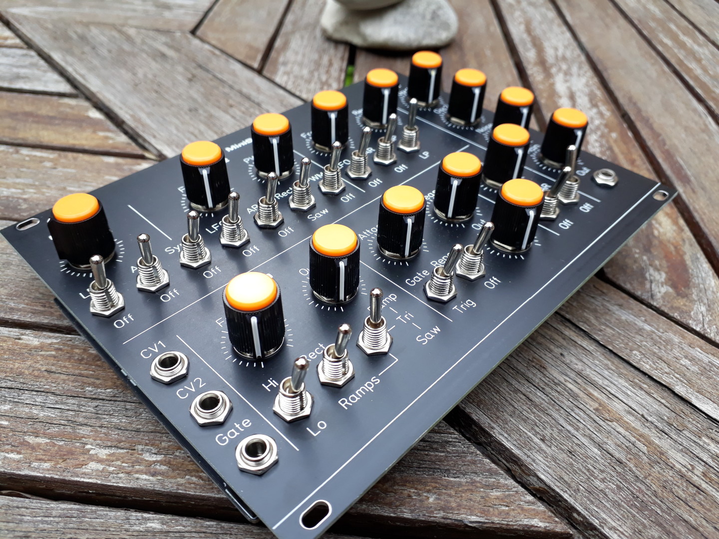
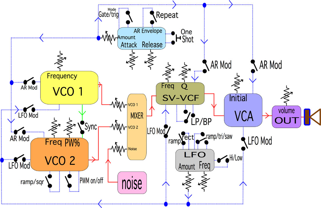
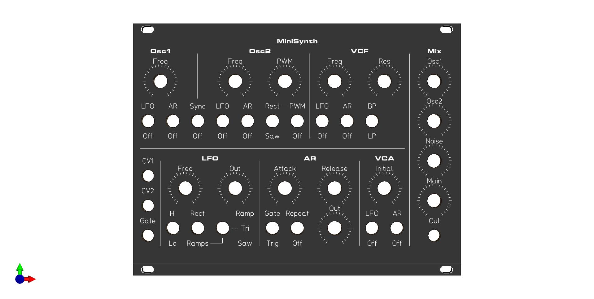
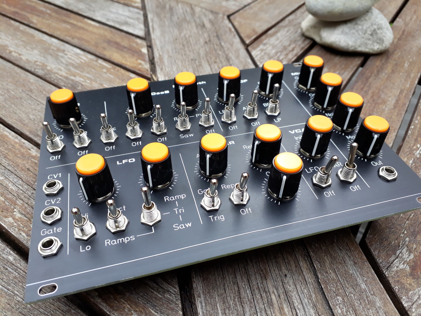
MFOS Sound Lab Mini-Synth is a cool analog monophonic synthesizer. The original version has been created by Ray Wilson from Music From Outer Space.
The SLMS is composed of:
- two VCOs (Saw and Saw+PWM),
- one Envelope Generator (AR, re trig-able),
- one LFO,
- one VCF,
- one VCA
- and one Noise source.
All the elements are internally routed. LFO and AR Envelope can modulate (On/Off) all the other elements.
See the diagram below for a graphical representation of the internal wiring.
Tom Fenn of Birmingham, UK. It will help you imagine the sounds you can make.”
(C) http://musicfromouterspace.com
You’ll find more details and explanations of the different circuits, the complete theory of operation, etc. on MFOS website.
The SMT Edition, version 1.4
The SMT Edition has been specifically designed to fit in a Eurorack System (Power input: -12, 0, +12 volts) and it removes any extra wiring. It’s a one board solution.
While the original was designed in Through Hole Technology (TH), this version is in Surface Mount Technology (SMT).
Some beginners might find that the Surface Mount Technology is more difficult to solder (smaller parts) than TH. But with a bit of technique and practice, SMT is as easy as TH, and maybe sometimes, easier. Besides, the SLMS uses the bigger 1206 size components. Those are easier to solder. Only two components use very small pin pitch and could be difficult to solder though. See below for details.
This project is, as for the original TH version, an intermediate project:
This project assumes a basic level of electronics proficiency and knowledge (…) and does not have step-by-step instructions to follow.
If you’re looking for a Through Hole PCB version, please have a look to MFOS website.
Same circuit…
The electrical circuit is identical to the original SLMS. Also, it includes some of the mods suggested by Ray: an improved Noise source and the improved Sync circuitry between VCO1 and VCO2.
I strongly recommend to read the original documentation.
Cross reference between the two versions is easy: the part references and values are identical. R1 in SMT version is R1 in Ray’s original version, and so on.
… with a few adaptations
The conversion from Through Hole to SMT required some component changes:
- The FET transistors (MPF102) Q5 and Q6 have been replaced by two BF545 or equivalents (MMBFJ310, MMBFJ211, MMBFJ202, MMBF4392LT1G, MMBFJ309LT1G and BFR31 have been tested ok).
- The four NPN transistors (2N3904) Q1, Q2, Q3 and Q4 have been replaced by two NPN arrays BC847BS. They are kind-of-matched and as the transistors in the array share the same package (different substrate though) they present an overall good thermal coupling.
Adaptation to Eurorack Power Bus is straightforward:
- The power input is connected through diodes D101 and D102.
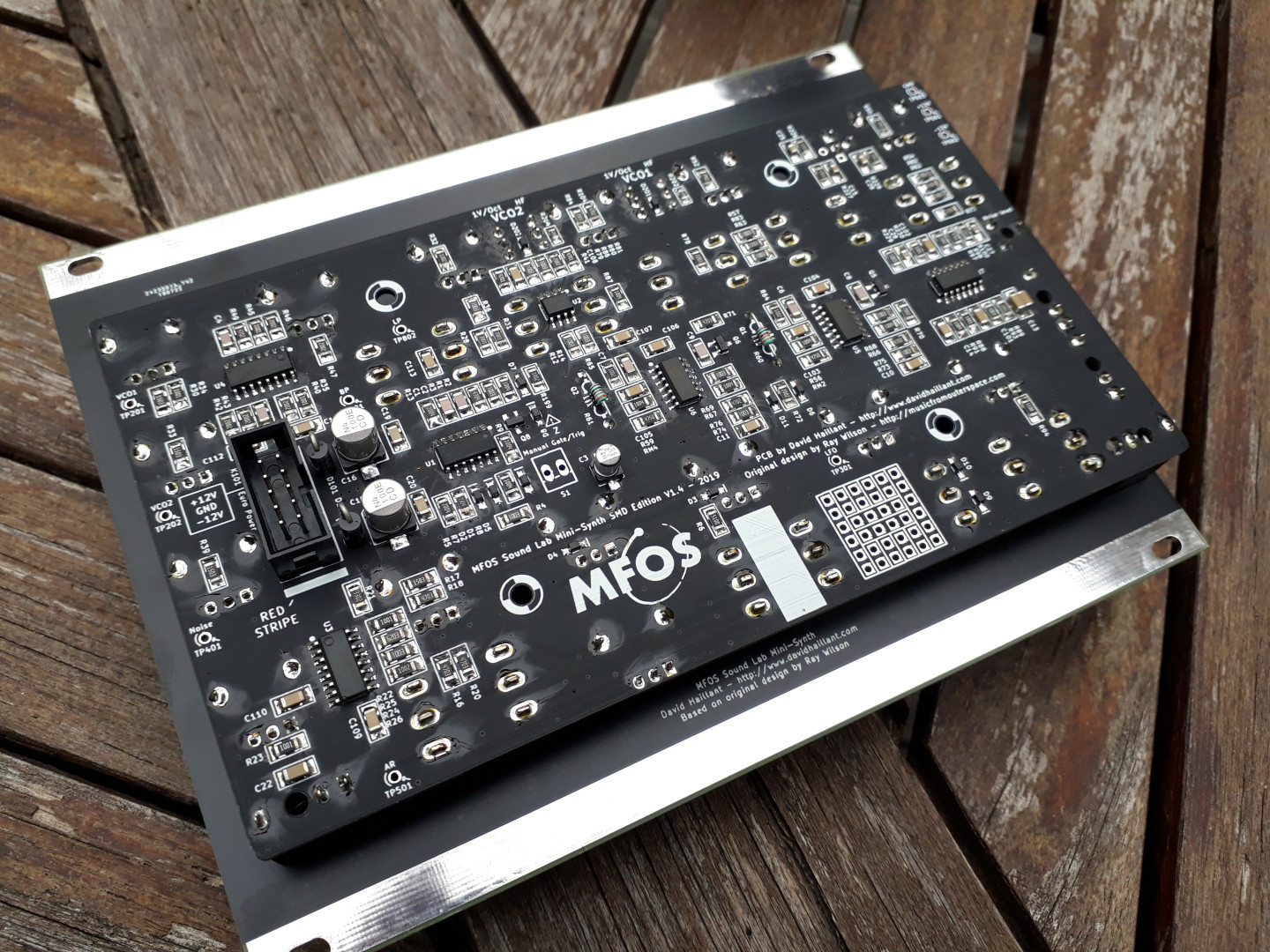
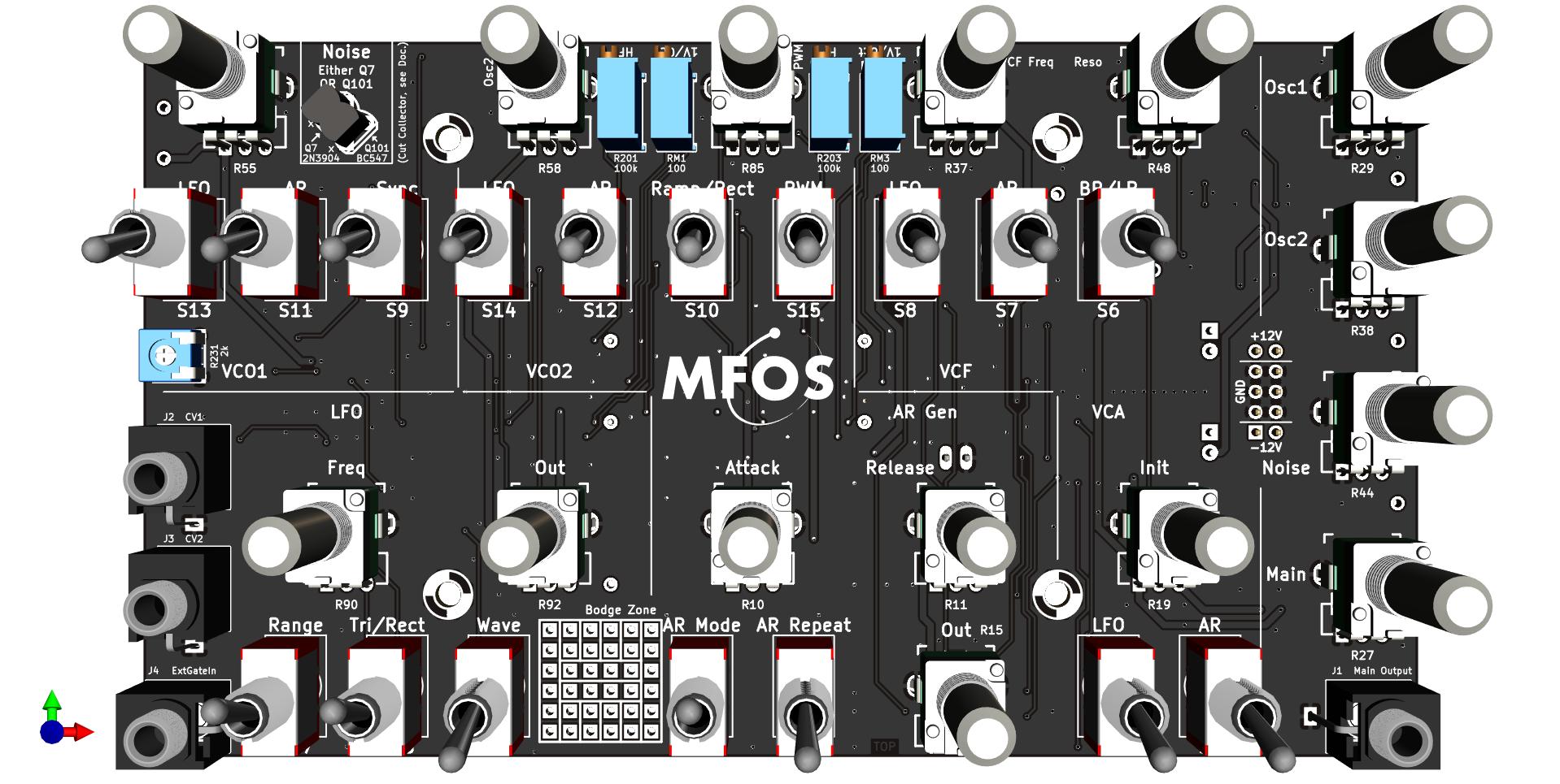
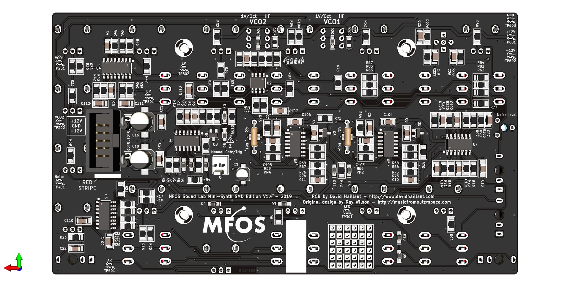
The PCB
The PCB is two layers, 1.6mm thickness, 160mm wide x 90mm high.
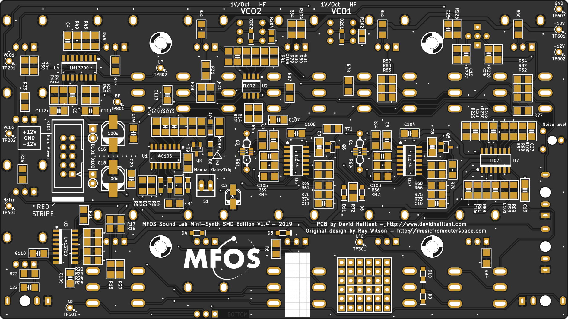
BOM
For a complete list of components, suggested sellers and parts, sorted by values, with refs and comments, see SLMS 1.4 Google Calc BOM document or below in Downloads section.
There’s also an interactive BOM available.
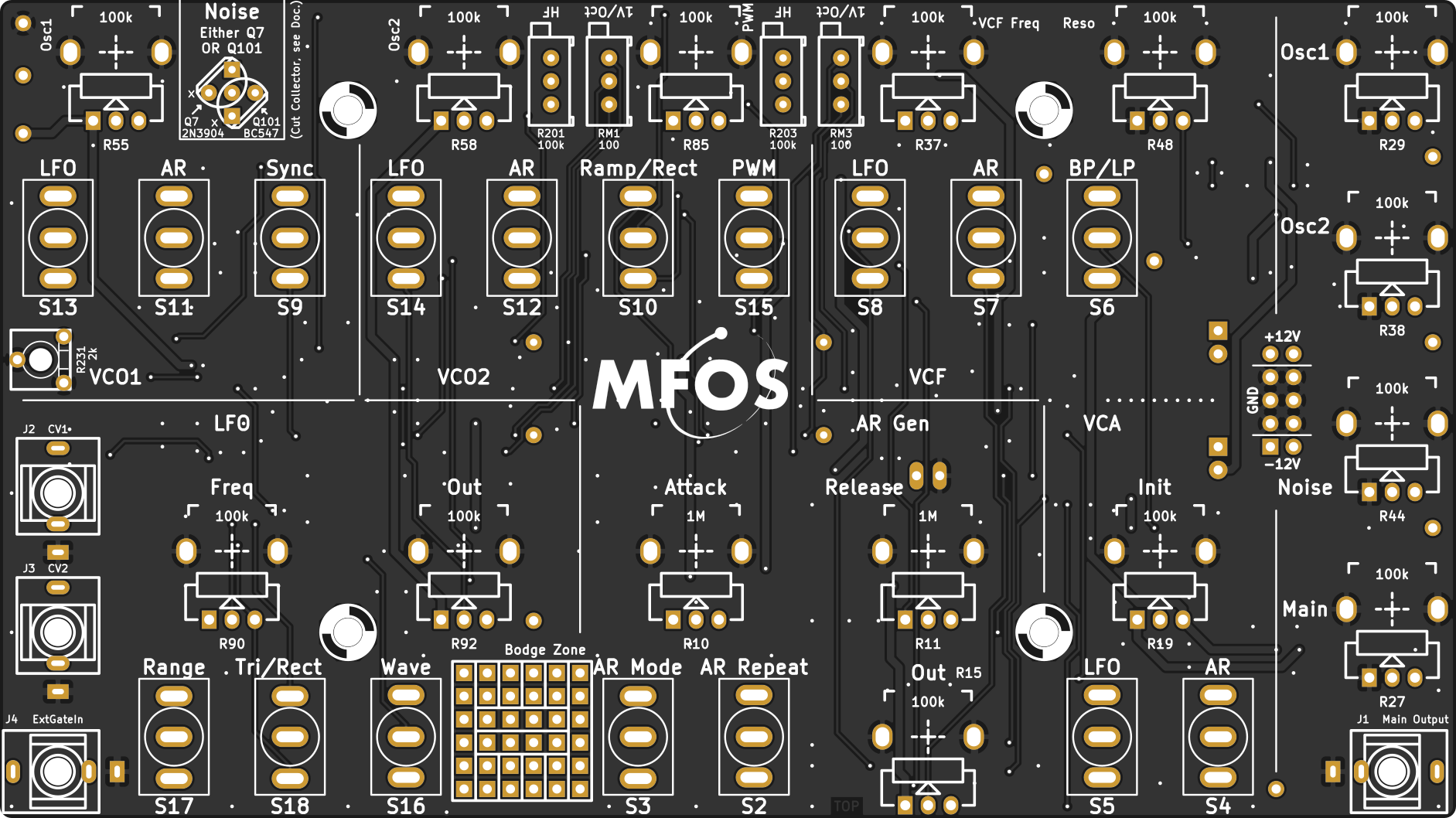
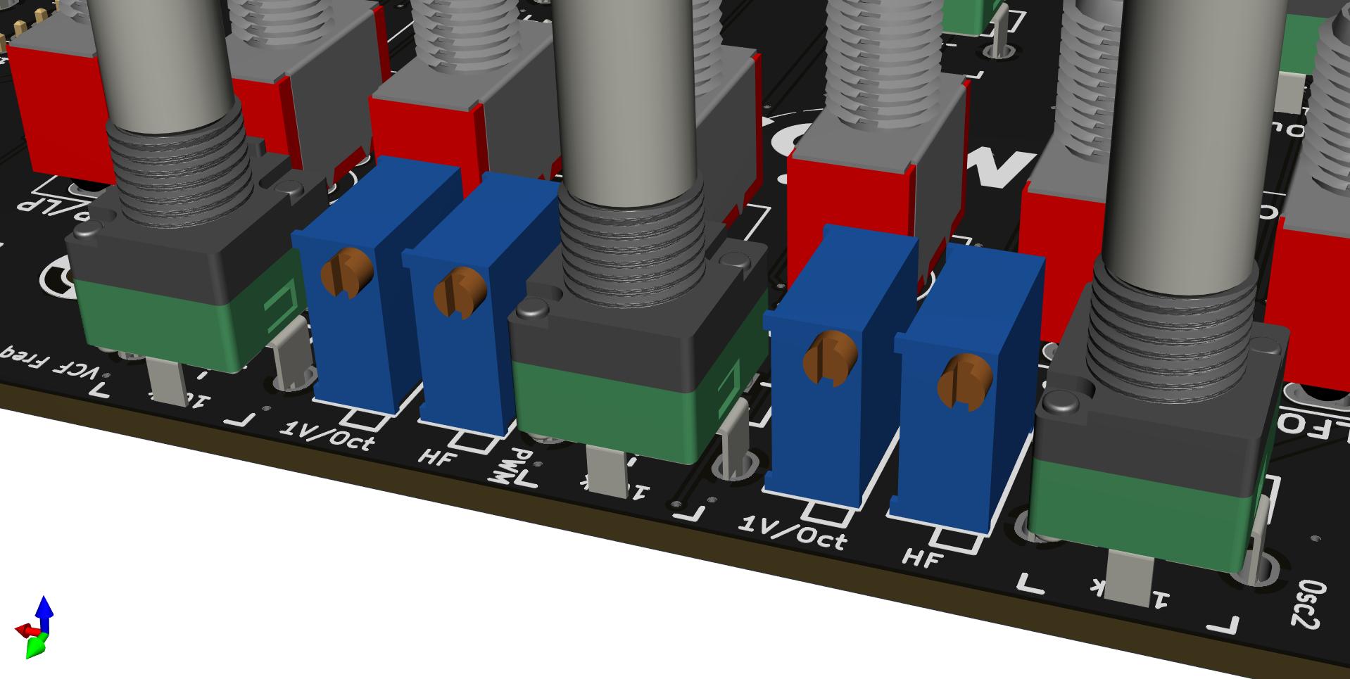
Temperature Compensation Resistors
Temperature Compensation Resistors R60 and R61 can be found at Thonk Tempco Resistor – Akaneohm 1% 3300ppm
However, it’s possible to use simple 50ppm/°C resistors instead. Your VCOs will work, track the 1V/octave CV input but will be out of tune as soon as the temperature will change.
Switches
All switches are SPDT (Single Pole, Double Throw) with the exception of S16, which is a “3 position On-Off-On” SPDT with an additional central position (No Contact).
SPDT is ON – ON (Mouser: 506-A101SYZQ04)
SPDT “3 position” is ON – OFF – ON (Mouser: 506-A103SYZQ04)
The two Mouser refs should be ok for the job.
Sources for pots and jacks:
Potentiometers:
- https://synthcube.com/cart/synth-diy/parts/potentiometers/alpha-9mm-potentiometer-right-angle-pcb-mount-6-35mm-round-shaft
- https://www.thonk.co.uk/shop/alpha-9mm-pots/
- http://smallbear-electronics.mybigcommerce.com/alpha-single-gang-9mm-right-angle-pc-mount/
- https://www.musikding.de/Pot-9mm-100k-lin-Print-vertical
10 mm height Jacks (PJ398SM / “Thonkicon”):
- https://synthcube.com/cart/synth-diy/parts/jacks/3-5mm-mono-jack-pj301m-12-hex-nut
- https://www.thonk.co.uk/shop/3-5mm-jacks/
- http://www.qingpu-electronics.com/en/products/WQP-PJ398SM-362.html
Suggested buttons:
- https://synthcube.com/cart/synth-diy/parts/knobs/knob-color-cap-black-w-white-index-6-4mm-shaft-13mm-diameter-set-screw
- https://www.musikding.de/Nose-Knob-orange
- http://smallbear-electronics.mybigcommerce.com/knurled-colored-caps/
Build instructions
The assembly process is simple. No kludge, bodge, correction, mod or anything else is required to make it operational.
The Surface Mount Components
SMT soldering is easier than what it looks like. No need for special tools or any special soldering iron or tip.
I recommend to use a thin solder wire. 0.3mm is good. 0.5mm is ok. And get a good pair of fine, non magnetic, tweezers.
The Interactive BOM/Pick and Place Map will help you with the placement of the SMT components. It is also a convenient tool if you need to debug your board. Click on any pad to highlight the other same net pads.
Usually, it is best practice to solder the smallest parts first. Taller components can block the access to other pads.
Start with ICs. The white dot marks on the PCB represent the pin #1. The thick bands represent the side with pin #1 and is also the side of the “slanted edge” on the SOIC packages.
Next step are resistors. Begin with the largest group of the same value resistors, for instance, the 100k group. Then continue with decreasing group sizes.
Tip: The resistors are not polarized, but it’s a good idea to place them in the same orientation, in order to be able to read the value codes without the need to rotate your board.
Ceramic capacitors come next. They aren’t polarized and they also have no markings to differentiate them. So do not mix the values! Work with one value at a time.
The ceramic capacitors require some special attention:
Ceramic caps are fragile. They can break easily if mechanically stressed, bent, twisted, squeezed, heated too much… You wont notice a broken cap, until it fails either open or worse, closed (short circuit!)
Continue with SOT transistors and SOD diodes. Prefer SOD 323 over SOD 323F. Attention, D8 is the Zener Diode.
The most challenging parts to solder are the two transistor arrays Q1 and Q2 (SOT 363 package). Fortunately, the BC847BS doesn’t have a polarity (the parts are in fact symmetrical) so just focus your attention on aligning correctly the pins to the PCB pads. Check for possible shorts between the pins. You can add flux before soldering, it will help the solder to flow correctly and it helps avoid solder bridges across the pads.
Finish with the aluminum (electrolytic) capacitors. Those caps are polarized. Align the PCB and the component markings.
The Through Hole Components
Now it’s time to solder the Through Hole Components. Here’s my recommended order:
Flip your board over.
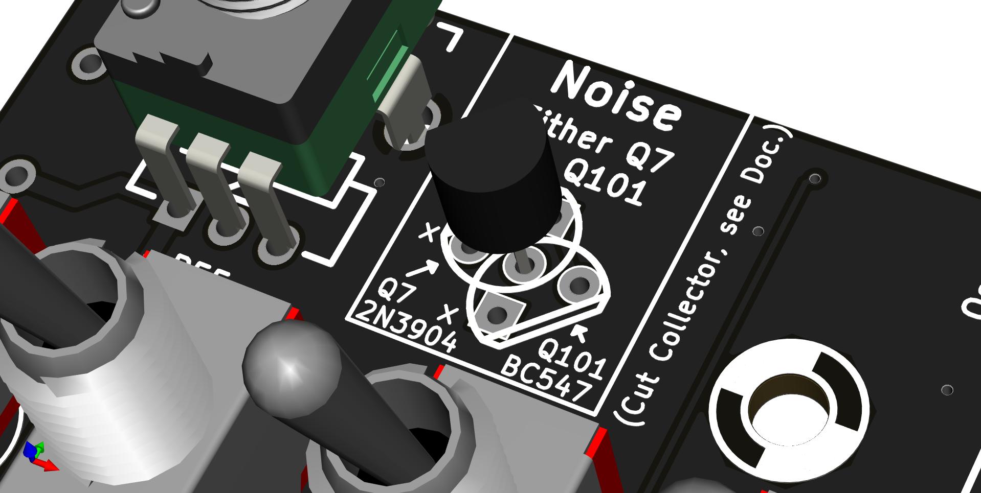
The noise source is a Through Hole transistor. Either Q7 (2N3904) or Q101 (BC547). 2N3904 (Q7) are good Noise sources. Use Q101 if you have BC547 instead. Use only one of them, not both.
Before soldering the noise transistor, you need to remove the collector pin. See the silkscreen indications: a small X shows which pin is to be removed, depending on the chosen transistor reference.
Then solder the noise transistor.
Flip back your board and solder the 10-pin Eurorack Power Connector K101. Pay close attention to the orientation. The connector must face the rear of the PCB (opposite to controls) and it is crucial to align pin #1. Pin #1 is represented by a small triangle on the silkscreen and an other small triangle on the shroud on the connector.
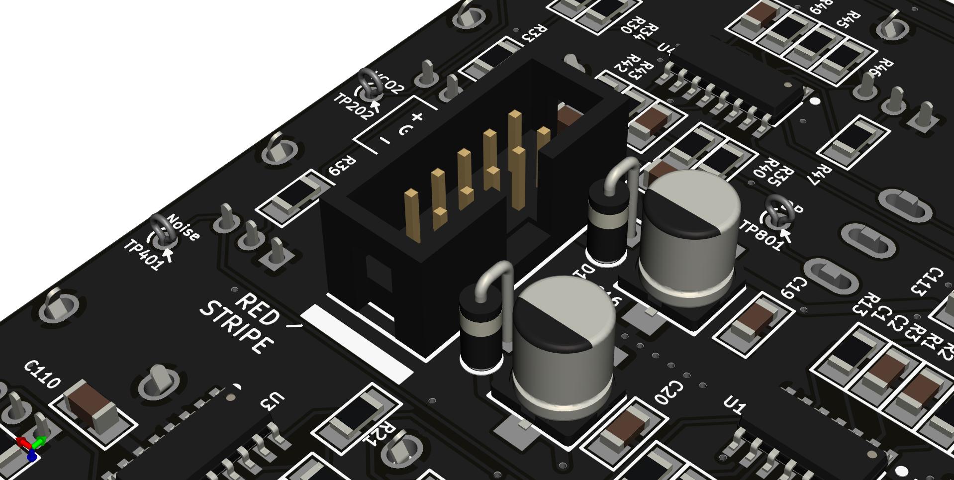
Note the orientation of the diodes, the capacitors and the 10-pin connector.
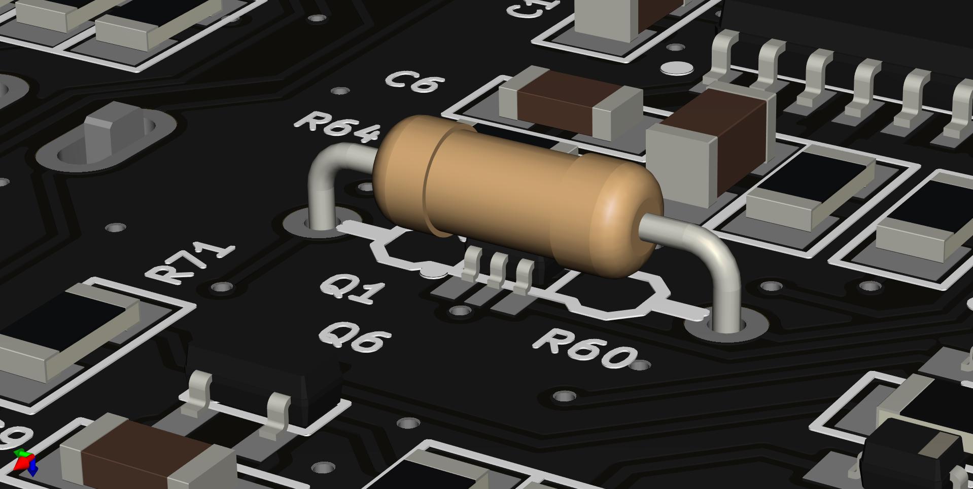
Now is a good time to solder the Tempco resistors R60 and R61. They are mounted on TOP of the Transistor Arrays Q1 and Q2. Place them in contact with the arrays. Use a small amount of thermal grease to improve the thermal coupling.
The Bottom side of the board is now complete (connector S1 is optional).
It’s time to solder the remaining TH components, starting as usual with the smaller ones.
The trim potentiometers RM1, RM3, R201 and R203 come first. Orient the screw heads toward the outside so that you’ll be able to adjust them once the front panel is in place.
If you already have the front panel, it’s best to use it now. It will help you align correctly the controls:
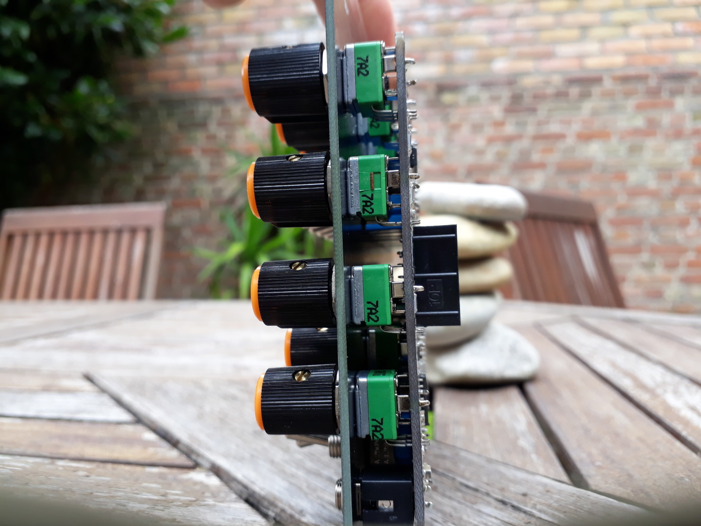
Place the four jack connectors, flip the board and, for now, solder only one pad of each.
Potentiometers may have a protruding tab that you must remove before. Use pliers to remove them.
Then, snap them in place on the PCB. Pay attention to the values: R10 and R11 are 1Meg Ohms. You might also need to remove the nuts and washers.
Solder only one of the two outer mechanical pins on each pot.
Now you can either first put in place the switches on the PCB, solder just one pin of each, then try to correct the alignment (inclination) while reflowing the solder. (you can use the front panel to help you in the process).
Or, highly recommended, you can simply bolt the switches to the front panel first and then position the front panel over the PCB and adjust the rotation of the switches so that everything fits nicely in place.
Pay attention to S16. It’s the only 3 position switch (On-Off-On). If your switches come with 2 washers and 2 nuts, keep only 1 of each.
Fasten some potentiometers in order to secure the front panel. Also fasten the jack sockets to correctly align them.
Once the front panel is in place and the controls are securely bolt, reflow the pre-soldered pins of the potentiometers, the switches and the jack sockets to release the tension on the pads.
Finally, solder the remaining pins.
Your board is now ready for the first tests and calibration.
Powering, First tests and calibrations
Before plugging in any power source, double check your job! If there’s a short circuit anywhere on the board, some damages can occur.
More important: Check the orientation of the polarized components.
To search for short circuits on the power rails, use an ohmmeter or a continuity tester on test points TP601, TP602, TP603. No value should be under few hundreds ohms.
Power your board with -12, 0, +12 volts (see “power connector” diagram on the board). A thick white band on the PCB indicates the -12V rail (usually the “red stripe” on your ribbon cable).
The -12V must not be confused with the 0V rail (also called “GND”). It’s a completely different voltage. See Ground is Not your Negative Rail on this subject.
Check the values again at TP601/TP603 and TP602/TP603. You should read values around +/-11V.
Plug a jack on the output socket. You should get a signal with switches on off position, VCO pots in mid position, VCF “Freq” pot on mid position, VCA pot on full clockwise, the mixer pots on full clockwise position.
For more information on how to test, debug and calibrate your synth, please read Ray’s original documentation.
The calibration procedure of the VCOs is covered in the original documentation.
The Front Panel
You can find the CAD file download link in the Downloads section below.
Downloads
- Schematics (mfos slms-1.4-20190825.pdf)
- Front Panel Express design, Black/natural engraving (euro slms 33hp 20180821.fpd)
- SVG version of Front Panel (euro-slms-33hp-20180821.svg)
- Front Panel dimensions (slms-33hp-20180821-dimensions-20200406.pdf)
- SLMS 1.4 Google Calc BOM document
Gallery
Please, send any comment or question!
Hello ! Je crois que tu parles français….. où est-ce que je pourrais acheter le module complet ou alors en kit ? Merci !
Your projects are phenomenal, with beautifully laid out boards and panels. KUDOS!
LOVED this one!
Got a not yet finished SoundLab mini and SoundLab Mk2 waiting for inspiration and a hot soldering iron, but this design intrigued me a lot.
However, being an elderly person dodging Corona virus and using a magnifying glass to read the numbers on “full-size” ICs, SMDs are definitely out of the question, but I have a very humble request:
Is it possible for you to share the Gerber files for this one. I am working a lot in a simple German program and I think I could “convert” your design to a design with hole-mounted components.
Next to solder SMD componets is miles of wire the worst thing there is.
Best regards
Magnus, Sweden
Do you where/if I can purchase a PCB for this project?
I turned on mfos sound lab today for the first time after I soldered it. It worked very well. Thanks a lot David.
Best Regards
Ali from Germany
Hi,
Congratulations for this job. Is it possible downloads Kicad Files ? or if not, purchase PCB ? An little question, why didn’t you intégrated S&H extension on your PCB ?
Best regards
Manuel
Bonjour Manuel, thanks for your kind words.
I’m sorry but I can’t share the KiCad files and all the prototype PCBs of the SLMS are all sold out now.
If you’re interested into getting the SMD version of the SLMS, please contact Synthcube (synthcube.com) who are now managing Ray’s legacy.
All the best,
David