The Simple VCO belongs to the same series as the Simple LFO.
It is a very stripped-down version of the Formant VCO, modified and adapted to the Eurorack format.
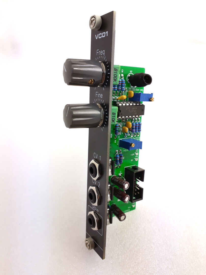
The Simple VCO is 1V/Oct capable. In order to reduce the number of parts, only one waveform output is available.
It is a very simple module, easy to build, understand, and maintain, yet fun to play and musically accurate.

Revision History
- V0.2 adds a “Fine” potentiometer. Some resistors have modified values. Check the BOM below.
- V0.2.1: C3 footprint changed from 2.54 to 5.08 pin pitch. This version is final and is a candidate for V1.0.
- V1.0 is the first official release.
- V1.1: Redesign of the frequency range controls for the Main and Fine potentiometers. Addition of diode D4 in series with D3 to minimize current leakage.
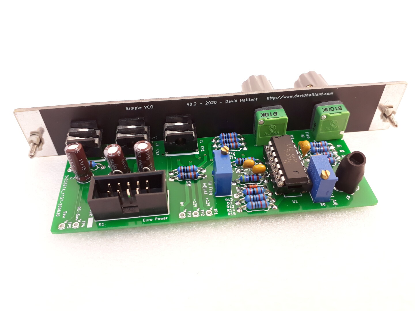
The circuit
The oscillator is a “saw core” VCO, derived from the Formant VCO. There are some differences, however: the comparator is an op-amp (U1B) instead of a CMOS gate, and the switching transistor has been replaced with diodes in series (D3 and D4).
Potentiometer R2 is the main frequency control. R4 defines the frequency range of the main potentiometer.
Potentiometer R18 is the fine frequency control. R19 defines the frequency range of the fine potentiometer.
The frequency is modulated by 2 external Control Voltages (CV): CV1 (J1) and CV2 (J2), through R5 and R6 respectively.
U1C is a summing amplifier. It sums the CVs and R7 is the 2k temperature-compensation feedback resistor. It is located close to the matched NPN transistor pair Q1 and Q2. R8 is responsible for adjusting the 1V/Octave tracking behavior. R11 is a high-frequency compensation trimmer. When the CV increases, the frequency tends to go flat. Adjusting R11 allows for better results at higher frequencies.
C4 is the capacitor where the sawtooth signal is generated: Q2 is a current sink and discharges C4 at a constant rate. U1A follows the voltage variation and U1B compares that value to a known voltage determined by R14 and R15.
The raw sawtooth signal (DC-Saw) goes roughly from +8V down to +3V. Around +3V, U1B triggers and sends a very brief positive voltage spike to the negative side of C4, through D3 and D4. This voltage variation quickly charges C4 and resets U1B, and the capacitor starts to discharge again.
It is important to note that the VCO relies at several points on the power supply rails for its voltage references. Any voltage variation on the rails will be noticeable in the frequency.


About the BOM
Many component values in the Simple VCO are not critical. It is a robust circuit that can tolerate many experiments and value modifications.
Resistors
| References | Value | Qty | 4-band Color Code | 5-band Color Code |
|---|---|---|---|---|
| R5, R6, R16 | 100k | 3 | Brown, Black, Yellow, Gold | Brown, Black, Black, Orange, Brown |
| R10, R14, R15 | 10k | 3 | Brown, Black, Orange, Gold | Brown, Black, Black, Red, Brown |
| R1, R9 | 1M | 2 | Brown, Black, Green, Gold | Brown, Black, Black, Yellow, Brown |
| R4 | 220k | 1 | Red, Red, Yellow, Gold | Red, Red, Black, Orange, Brown |
| R12 | 22k | 1 | Red, Red, Orange, Gold | Red, Red, Black, Red, Brown |
| R19 | 2M2 | 1 | Red, Red, Green, Gold | Red, Red, Black, Yellow, Brown |
| R7 | 2k Tempco | 1 | Red, Black, Red, Gold | Red, Black, Black, Brown, Brown |
See Resistor color code chart.
Tempco R7
R7 is a 2kΩ, 3300 PPM Positive Temperature Compensation Resistor. It is not an NTC (Negative Temperature Compensation).
If you can’t get a proper Positive Tempco, you can simply use a plain resistor. However, 1V/Oct tracking will drift due to temperature changes.
C5 and C6
The 2 input capacitors C5 and C6 can have any value between 1µF and 100µF. A common value is 10µF. One important consideration is the minimum operating voltage of C5 and C6: it must not go below 25V.
Potentiometers
(Links may not work, please report any issues.)
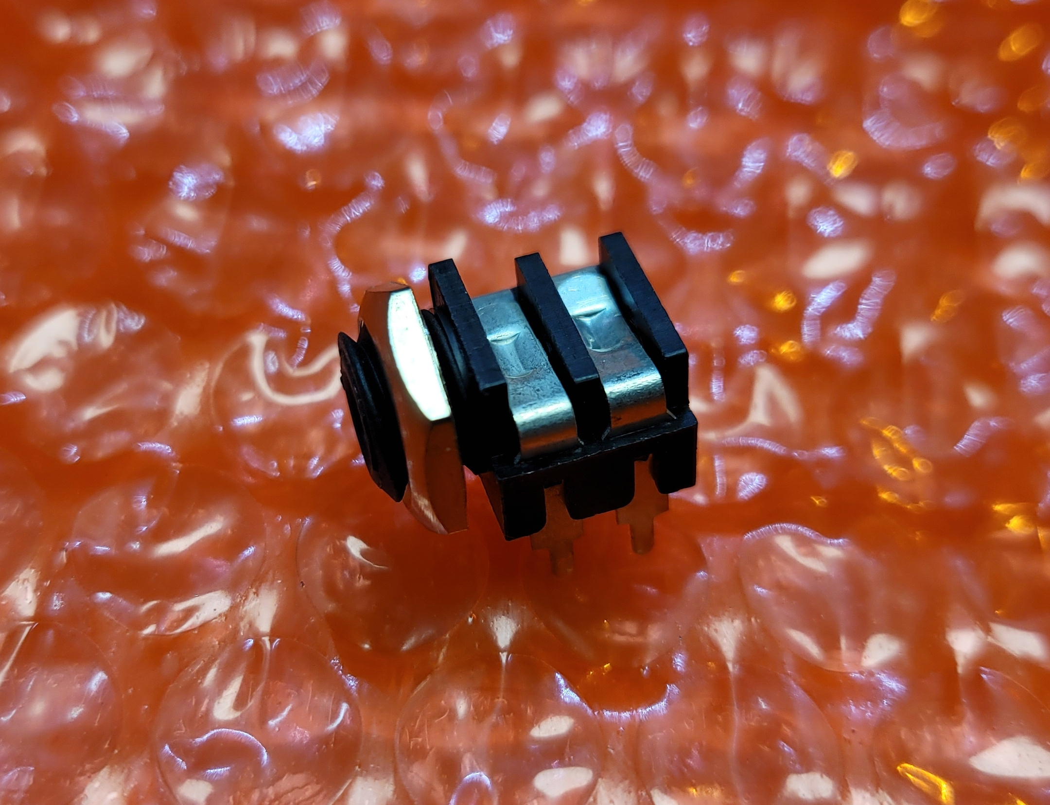
Jack connectors
The jack connectors are Cliff CL1384.
About the diodes D1, D2, D3, and D4

D1 and D2 are protection diodes: they protect against reversed voltages on the power connector. They can be bypassed with wire jumpers or clipped component legs.
They are to be mounted vertically, over the circle printed on the PCB, with their cathode pin pointing up. The cathode side of the diode is the one with the white ring.
In other words, the Cathode must be connected to the square pad while the Anode is connected to the round pad.
D3 and D4 inject the reset pulse that allows the capacitor to recharge: this is the moment when the waveform transitions from a linear downward slope to a near-instantaneous rise, producing the characteristic sawtooth shape. D4 was added in V1.1 to minimize potential current leakage through D3 by placing two diodes in series. This approach is inspired by the VCO4 design by Schmitzbits.
Calibration and first tests
Powering on
Once you believe you have soldered everything correctly, and before powering your module for the first time, check TWICE that nothing is mounted backward and that the power input connector is correctly oriented, and that your power cable is trustworthy!
Then, CHECK AGAIN!
Furthermore, it is recommended to power the module for the first time without any IC inserted and to check, with a multimeter, the presence of the expected voltage rails on the correct pins.
VCO calibration
The calibration process is identical to that of any other VCO. The multi-turn trim potentiometer R8 sets the 1V/Octave conformance.
The second multi-turn trim potentiometer, R11, is the setting for the high frequency compensation.
The required tools are:
- An accurate voltage source capable of delivering CV in 1V steps (0V, 1V, 2V, etc.): a CV keyboard or a MIDI-to-CV module.
- A frequency meter or a tuner.
- A small flat-blade screwdriver.
- Your tongue at the right angle and some patience.
- Also a multimeter, because you always need a multimeter.
- And if you have an oscilloscope, it is a good idea to monitor the waveforms.
R11 must first be set to the lowest resistance between pins 1 and 3 (fully counter-clockwise position).
The oscillator frequency can also be read from test points TP4 and TP5.
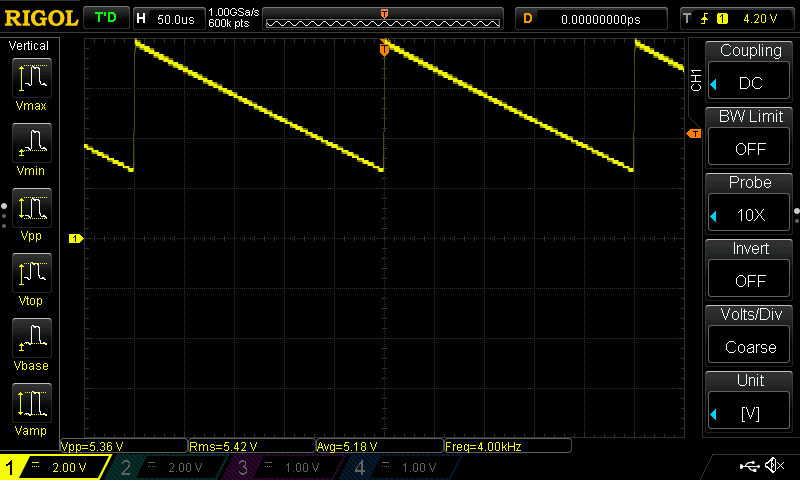
- Apply no CV input (0V) and turn potentiometers R2 and R18 to set the oscillator frequency to a low value. With a frequency meter, set it to an easy-to-read value such as 100 Hz. With a tuner or by ear, tune precisely to A2 (110 Hz).
- Apply a 1V source on the CV input. The frequency of the oscillator should double (200 Hz or A3). If the frequency is flat, adjust trim potentiometer R8 to bring it slightly flatter. If it is sharp, adjust R8 to bring it slightly sharper.
- Return to 0V on the CV input. The frequency is no longer exactly 100 Hz (or A2). Adjust R18 back to precisely 100 Hz (or A2).
- Repeat step 2 until the frequency doubles exactly when 1V is applied to the CV input.
- Check that the VCO frequency doubles again with a CV of 2V. The frequency must be 4× the base frequency (400 Hz or A4).
- Do the same for 3V, 4V, etc. The frequency must double for each additional volt applied to the CV input.
- At some point, the frequency will start to go flat regardless of how precisely the VCO was tuned on the lower octaves. Adjust trim potentiometer R11: turn it clockwise to increase the frequency. Once back in tune, return to step 2 and start again.
After several iterations, the VCO can stay in tune across multiple octaves. The number of in-tune octaves depends on several factors, including the quality of the transistors. Note that transistor matching affects temperature drift correction, not the tuning accuracy itself.
Drawings and dimensions


Videos
Brilliant stuff! V/Oct on a single TL074, very cool.
Thank you 🙂