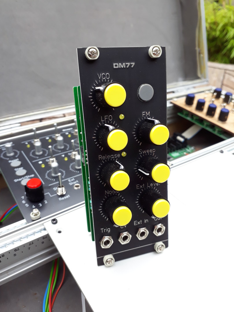
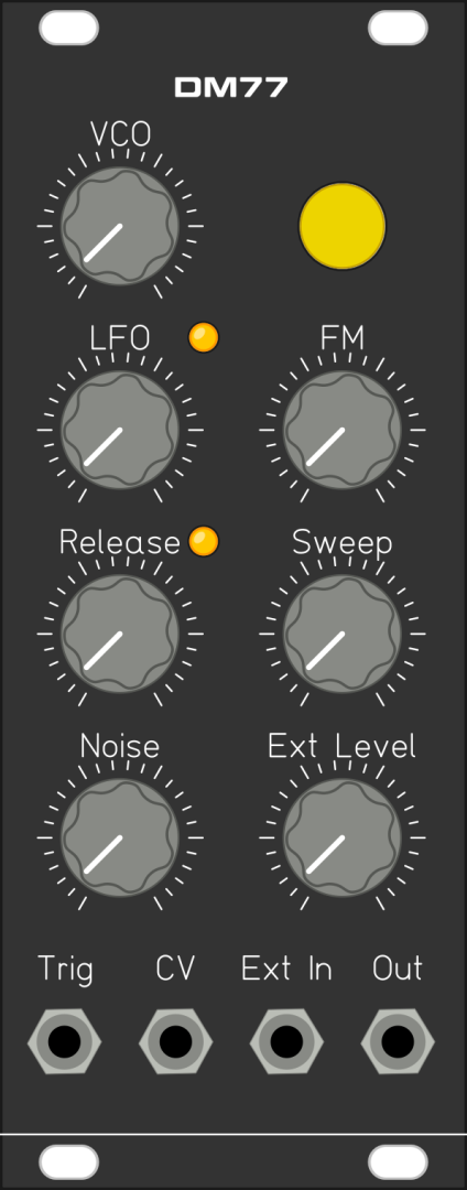
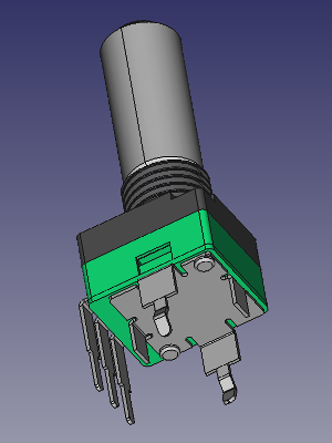
The DM77 is a Drum Synthesizer, inspired by the Coron DS8, with improved characteristics.
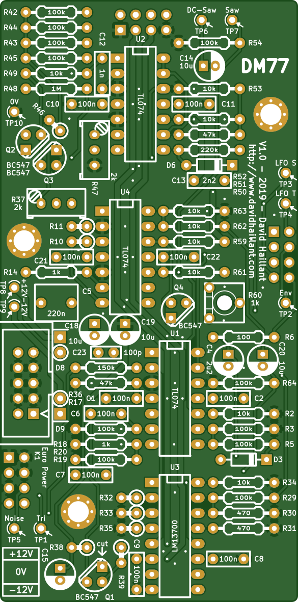
Revision 1.0 of the Front board contains an error!
This problem has been corrected in revision 1.0b
A trace creates a short circuit at LED D4 (Envelope): The square-shaped pad of D4 (cathode) is in contact with the trace coming from the second pad of D4 (anode).
The consequence is that the two pins of D4 are connected together, which then prevent the Envelope LED to light up.
If you have a board revision 1.0 with this error, please read Assembly guide.
Description
The main oscillator produces a triangle waveform. The frequency range goes from sub-audible to ultrasonic. The Sweep effect follows the envelope signal and modulates the frequency of the main oscillator. The second oscillator, a triangle LFO, also modulates the frequency of the main oscillator through the FM setting.
The Noise potentiometer sets the amount of white noise in the final signal. The “Ext” circuitry allows to add an external audio source to the final signal.
And finally, the output signal is controlled by a VCA, following the envelope (Release/Decay setting).
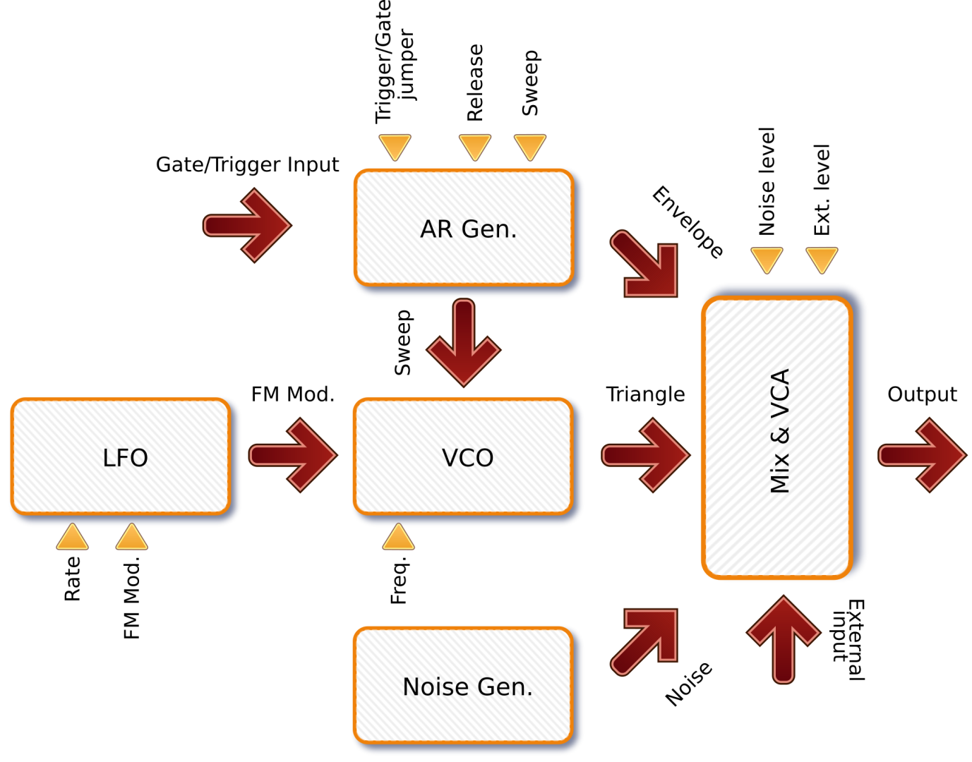
In details
The circuits described below are derived from several well-known synth circuit blocks, adapted or modified for the DM77. Most of the circuits, including component values are subject to modifications or improvements, and I strongly encourage, anyway, to experiment, hack, transform, modify whatever you want!
The VCO

The main oscillator is a “saw core” VCO, derived from the Formant VCO. There are some differences though: the comparator is an op amp (U2D) instead of a CMOS gate, and the switching transistor has been replaced with a simple diode (D5).
Potentiometer R13 is the main frequency setting. R40 and R41 define the upper and lower limits of the base frequency range.
The frequency is modulated by 3 Control Voltages (CV): Ext-CV, Sweep and LFO, through R42, R43 and R44 respectively.
U2B is a summing amplifier. It sums the CVs and R46 is the 2k temperature-compensation feedback resistor. It is located close to the matched NPN transistor pair Q2 and Q3. R47 is responsible for adjusting the 1V/Octave tracking behavior. R37 is a high frequency compensation trimmer. When the CV increases, the frequency tends to go flat. Adjusting R37 allows to get better results on higher frequencies.
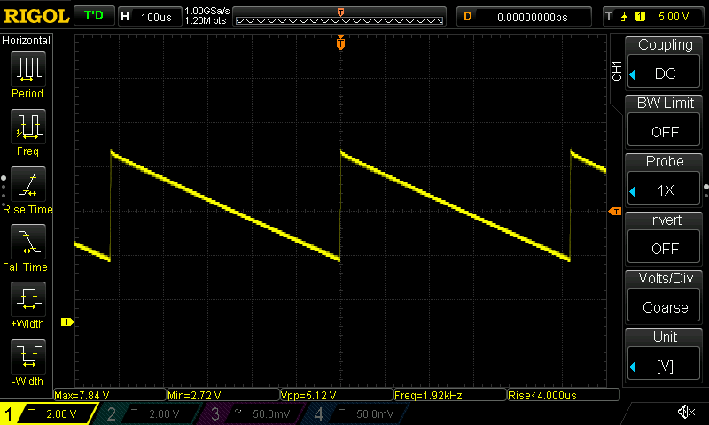
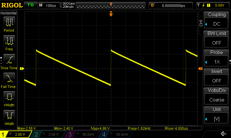
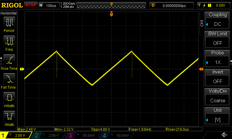
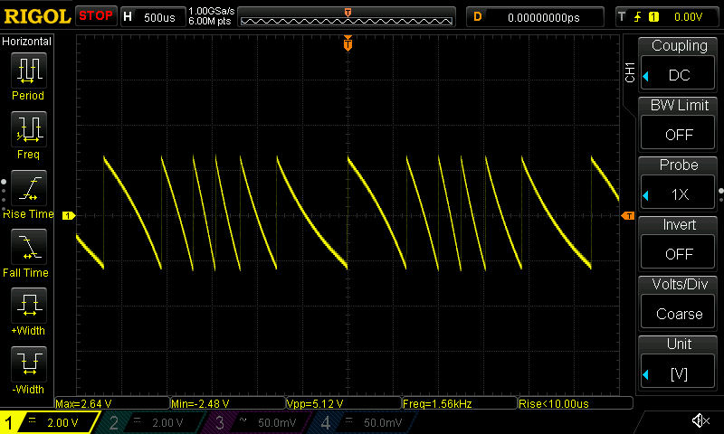
C13 is the capacitor where the saw tooth signal is generated: Q3 is a current sink and discharges at a constant rate C13. U2D follows the voltage drop and U2C compares that value to a known voltage determined by R52 and R53.
The raw saw tooth signal (DC-Saw) goes roughly from +8V to +3V. Around +3V, U2C triggers and sends a very brief positive voltage spike to the negative side of C13, through D6. This increase in voltage quickly charges C13 and resets back U2C and the capacitor starts again to discharge.
It is important to note that the VCO relies at several places on the power supply rails for its voltage references. Any voltage variation on the rails will be noticeable in the frequency.
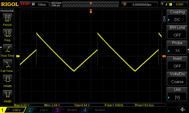
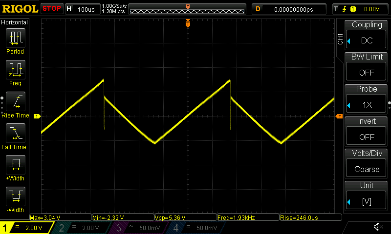
The waveshaper
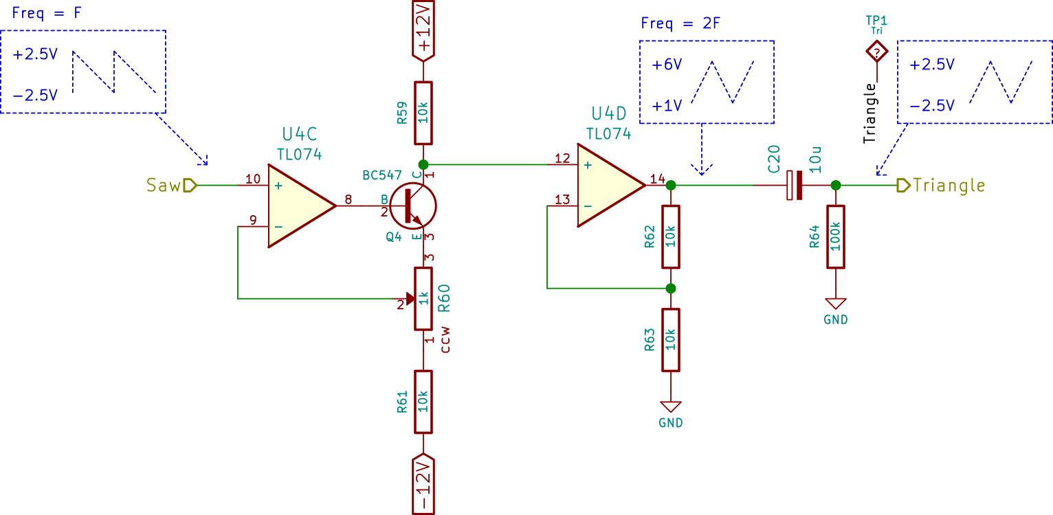
The AC saw tooth signal is then fed to the triangle waveshaper U4C and D. The negative portion of the saw waveform is rectified and becomes positive. The resulting signal needs to be adjusted to get a correct triangle waveform. The trim potentiometer R60 cancels the offset between the positive and negative portions and then removes some remaining artifact glitches. The glitch adds some high frequency harmonics an can be kept for more “sound characteristics”.
The triangle signal is 5V peak to peak. And times two the initial saw tooth signal frequency.
The input stage
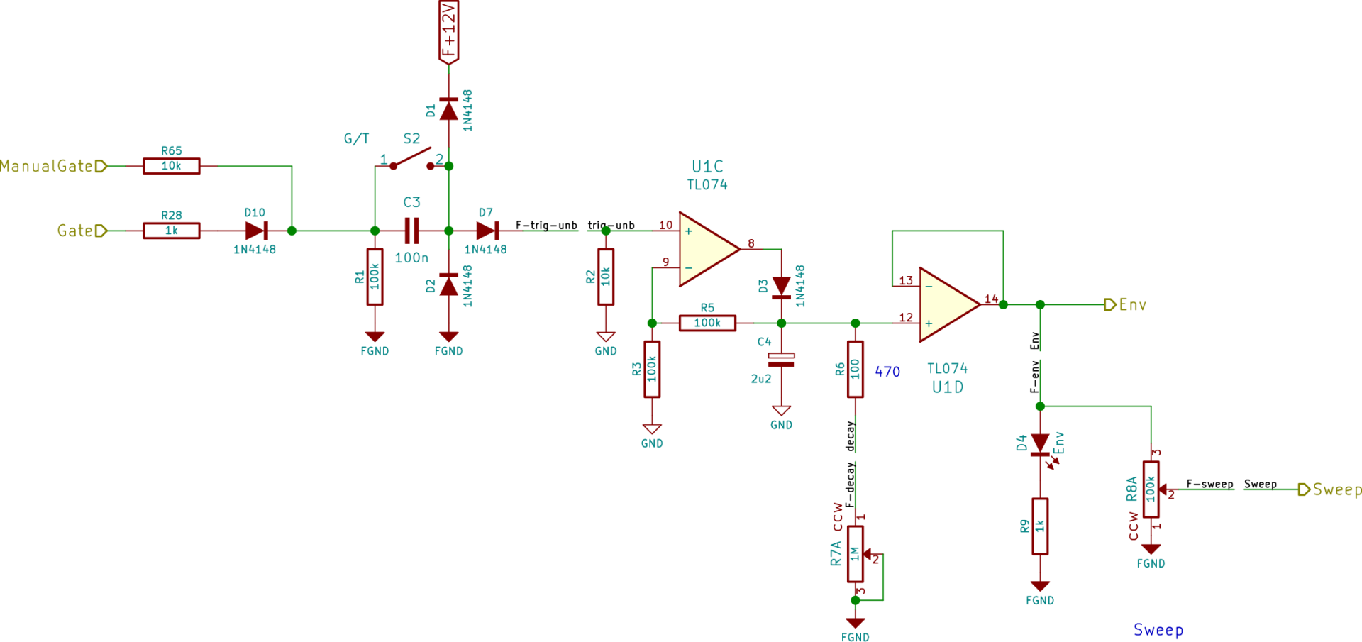
The Gate/Trig signal is fed through several passive filtering components to U1C. Diodes D1, D2 and D3 remove the negative portion of the input Gate signal. They also clip the excess voltages.
If switch S2 is open, C3 converts the gate signal to a trig signal. If S2 is closed, C3 is bypassed.
U1C greatly amplifies the gate/trig signal to ensure that even small positive voltages can be effectively detected.
C4 charges immediately when D3 is forward biased by U1C. Then, C4 slightly discharges through R6 and the potentiometer R7. The discharge rate is set by R7. U1D follows the voltage on C4 and provides the envelope signal to the VCA. The LED D4 is ON when the envelope signal is present and fades away when it disappears.
R8 is the Sweep potentiometer. It sends a portion of the envelope voltage to the VCO for a sweep modulation effect (from high to low frequency).
The LFO
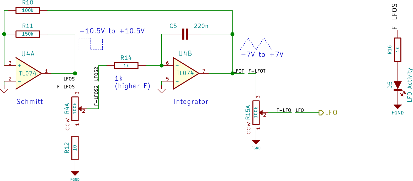
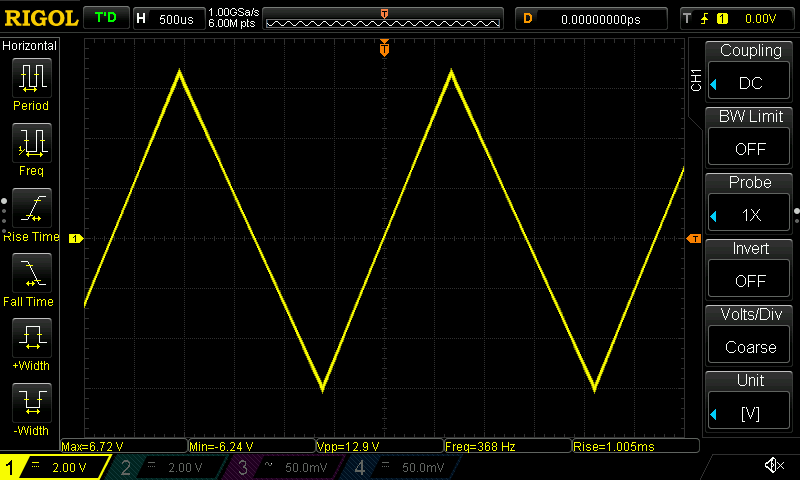
The second oscillator is a simple triangle waveform LFO. The potentiometer R4 sets the rate. U4A is a Schmitt trigger comparator and U4B is an integrator. Capacitor C5 charges or discharges linearly at a rate defined by the position of R4.
Once LFOT signal reaches a defined voltage level, the Schmitt trigger swings its output (LFOS) to either +10 or -10V.
The potentiometer R15 “LFO Mod.” sends a portion of LFOT signal to the VCO as a Control Voltage for FM modulation.
LED D5 blinks at the rate of LFOS. D5 can be a Bi-color LED, and change of color according to the sign of the LFO waveform (positive or negative).
The noise source
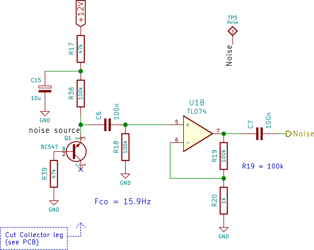
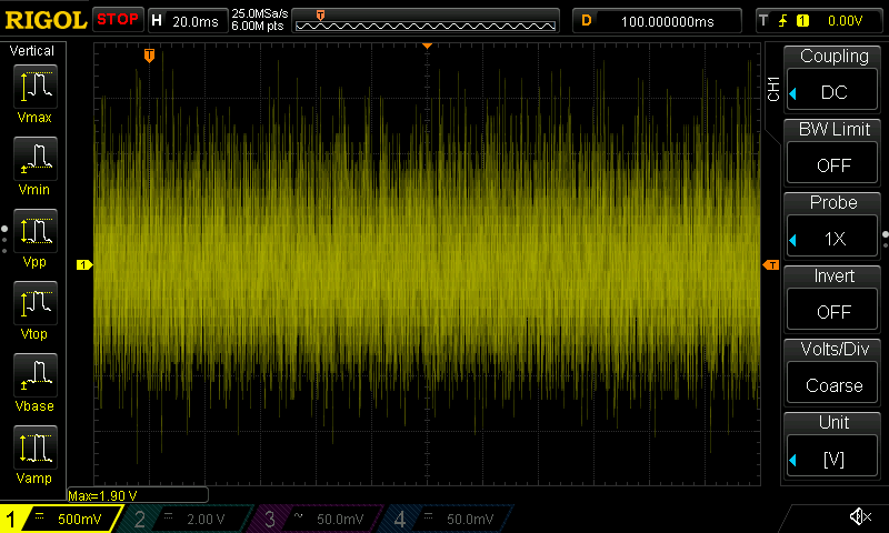
The white noise is produced by Q1, a reverse biased NPN transistor. U1B amplifies the noise signal to a useful level. It may be necessary to adapt that level by modifying the value of the feedback resistor R19. Values can range from 10k for a noisy transistor to 1Meg for a very quiet Q1.
The network composed with C15, R17, R38 and R39 eliminates the interactions between the power supply rails and the noise transistor. The noise signal is immune to power supply variations and the power supply rails aren’t polluted with white noise.
C6 and R18 form a Hi Pass filter.
Collector leg of Q1 is to be cut before soldering. See the PCB for identifying the pin #1. Cutting the collector leg reduces the risk of picking up HF content.
The VCA
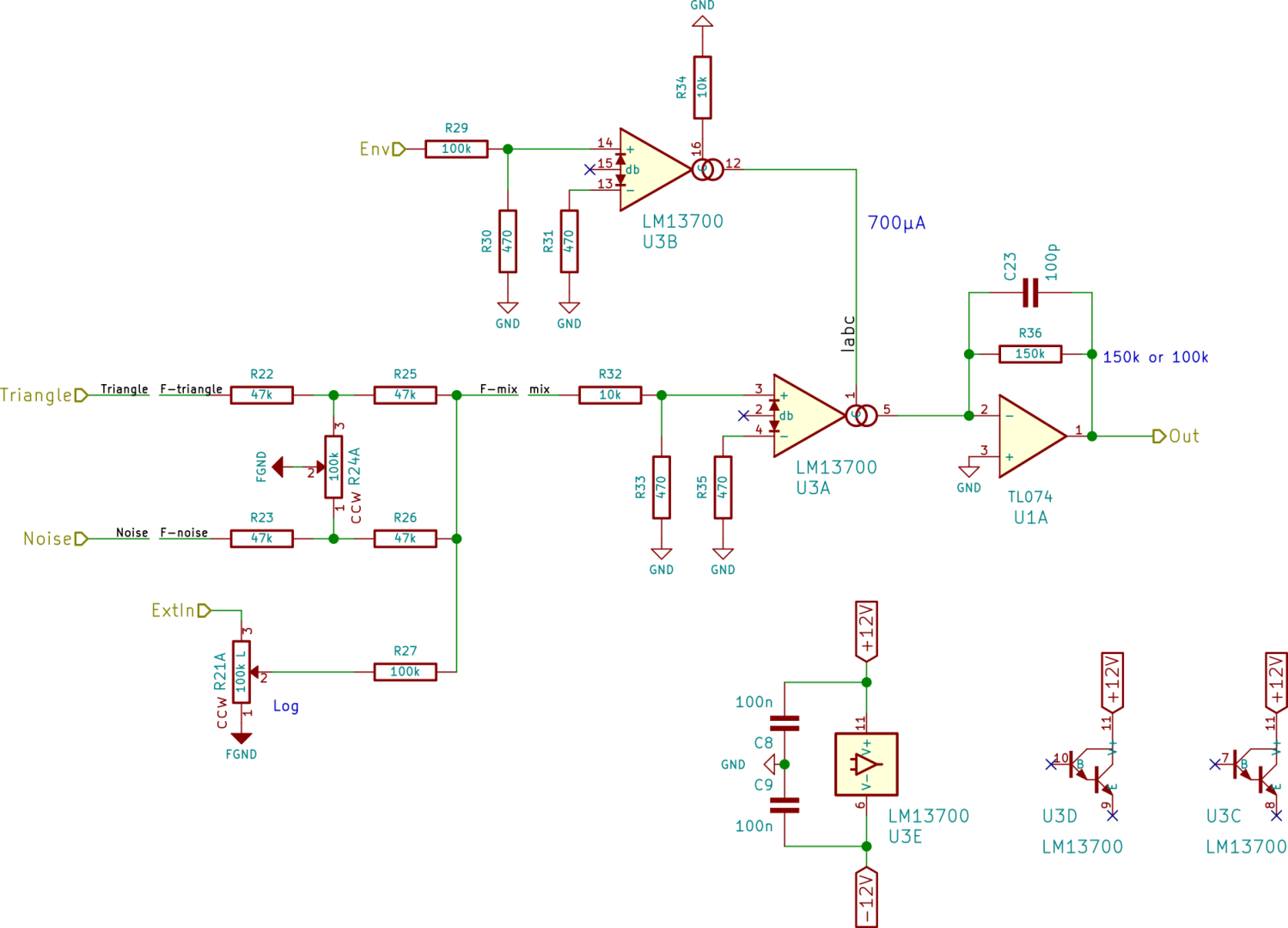
The Voltage Controlled Amplifier is the last stage in the path for signal of the DM77.
The signals from the VCO, the noise generator and from the external audio input are mixed together at R25, R26 and R27 common node (F-mix). R24 sets the balance between the triangle and the noise signal. R27 can be adapted for the external input signal needs.
U3 is an OTA. The gain of the VCA is set by “Env”, the envelope signal. The envelope voltage is converted to a current (Iabc) by U3B and then fed to U3A. Iabc modifies the gain of U3A.
U1A converts the current at the output of U3A to a voltage. R36 sets the level of the output signal. Use a lower value for line level signal.
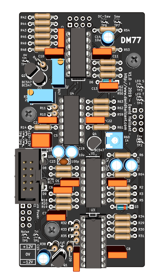
See the schematics in “Documentation” section below.

Simulations
Component selection
All the components are Through Hole.
Resistors
The resistors are 1/4W carbon film or metallic.
R46 can be a simple 2k2 metallic resistor for a basic VCO, that will drift with temperature changes.
To reduce the temperature drifts, use a linear positive temperature coefficient resistor. Thonk has a nice Akanehom 2k 1% 3300PPM tempco resistor.
Trimmers are vertical 25 turns 3/8″ trim pots. Inline pins. Screw on top.
Capacitors
The small value capacitors are either ceramic or film/polyester, but for best performances, the VCO timing capacitor C13 should be a film/mica/polyester/polystyrene capacitor.
They are 5mm lead spacing. Except C23 who is 2.5mm pin pitch.
Bigger capacitors are Electrolytic (Aluminum) caps with a pin pitch of 2.5mm.
They must be rated 25V minimum. C14 and C20 can be either polarized or bipolar.
Active parts
Use sockets for ICs. I prefer the machined ones, but other types are ok.
The transistors are BC547 or equivalent pinout NPN bipolar transistors.
Q2 and Q3 need to be matched for good 1V/Oct tracking over a wide temperature range.
Note that, the ability to follow the 1V/Oct behavior doesn’t depend on the matching of the transistors, nor the tempco resistor. Those parameters are only useful for temperature drifts.
LEDs
The LEDs are preferably 3mm in diameter.
D5 can be a bi color LED and be on always, only changing color with each LFO’s polarity alternance. D4 is single color only, as the Envelope signal is positive only.
I use the following references:
- L-934LYD (yellow LED)
- L-937EGW (bi color Red/Green LED) – useful only for LFO
It is possible to change the LED protection resistance to adjust its brightness or reduced power consumption. For more brightness, 430 Ohms is the reasonable lowest value (less than 20mA with 10V supply and a 2V Vf LED). 1k is a compromise between current consumption and brightness. For very low current LEDs, 3.9k might be ok (To be tested).
Jack sockets
You can find the Thonkiconn jack sockets here:
- Thonk (https://www.thonk.co.uk/shop/3-5mm-jacks/)
- Synthcube (https://synthcube.com/cart/synth-diy/parts/jacks/3-5mm-mono-jack-pj301m-12-hex-nut)
Potentiometers
You can find the potentiometers here:
- Thonk (https://www.thonk.co.uk/product-category/potentiometer/)
- Synthcube (https://synthcube.com/cart/synth-diy/parts/potentiometers)
- Tayda (https://www.taydaelectronics.com/100k-ohm-linear-taper-potentiometer-round-shaft-pcb-9mm.html)
The potentiometers are all linear, except R21, who is dealing with audio signal, so Log is a better choice. This parameter is not critical though.
The decay/release R7 is 500k, but you can use a 1Meg for longer sounds, or a 100k for shorter sounds.
You can also use different values for C4: Smaller capacity = shorter sounds.
Push button
The manual Trig/Gate push button S1 is a model D6 from C&K. See Thonk (https://www.thonk.co.uk/shop/radio-music-switch/)
Component value changes
To date, no changes required in version 1.0.
Assembly guide
This problem has been corrected in revision 1.0b
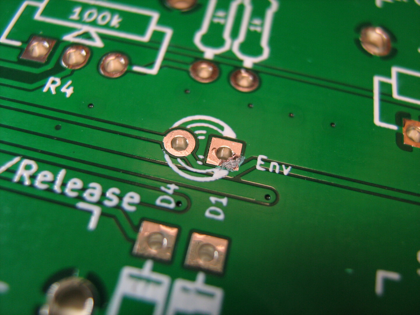
The easiest way to correct this is, with a sharp tool, to cut the corner of the pad in contact. Be careful not to cut the trace itself.

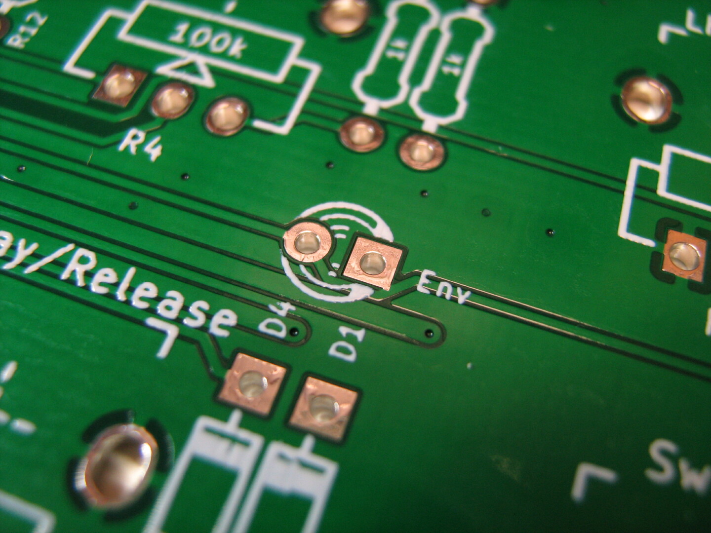
Also please note that, on some PCBs, the label “D4” is misplaced. D4 is the LED. D1 label is correctly placed. Diode D7 is located between potentiometer R7 and diode D1. Its label is missing.
To verify that the square pad of D4 is no longer in contact with the adjacent trace, use either a continuity tester or an ohmmeter at the LED’s pads. No continuity should happen here.
Also, some users reported they connected directly the cathode pin of D4 to R9. If you don’t feel at ease modifying the PCB, you can use this method instead.
R9’s leg needs to be de-soldered first and you need to avoid contact from the pad.

If you need help, please contact me.
Building the DM77 is pretty straightforward. It only consists of easy-to-find, classic, Through Hole, components.
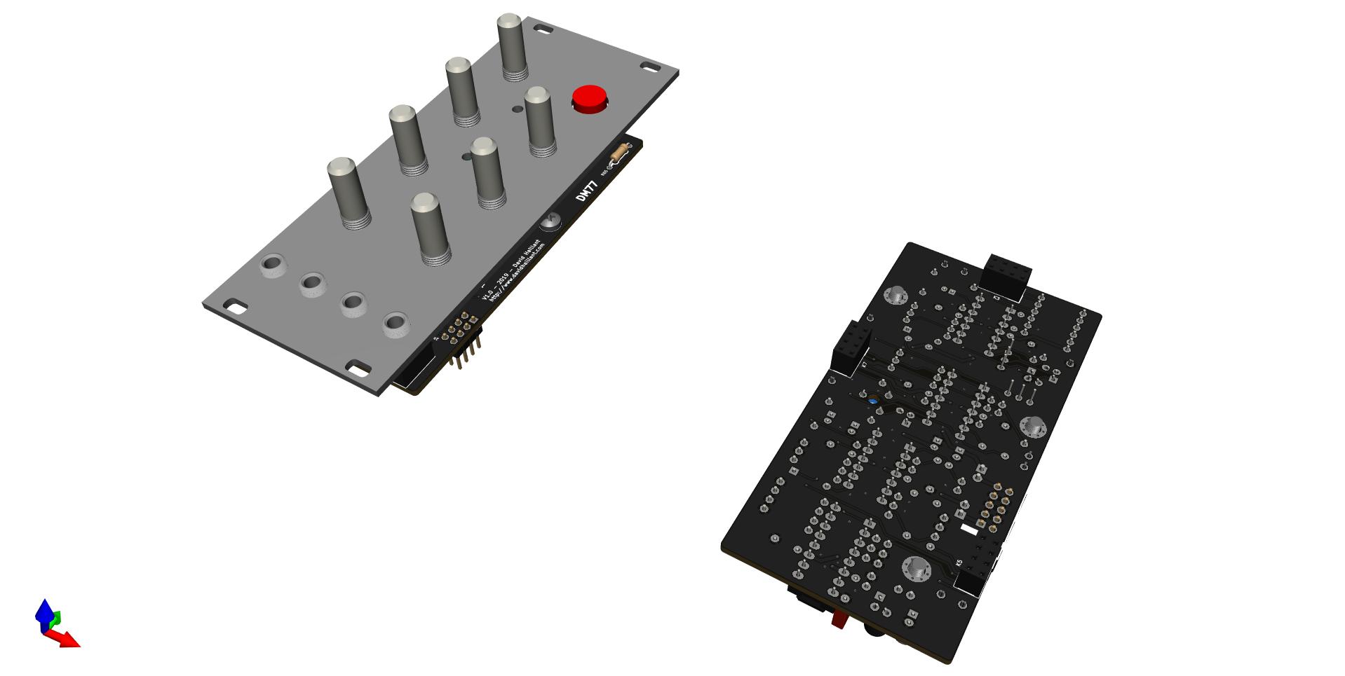
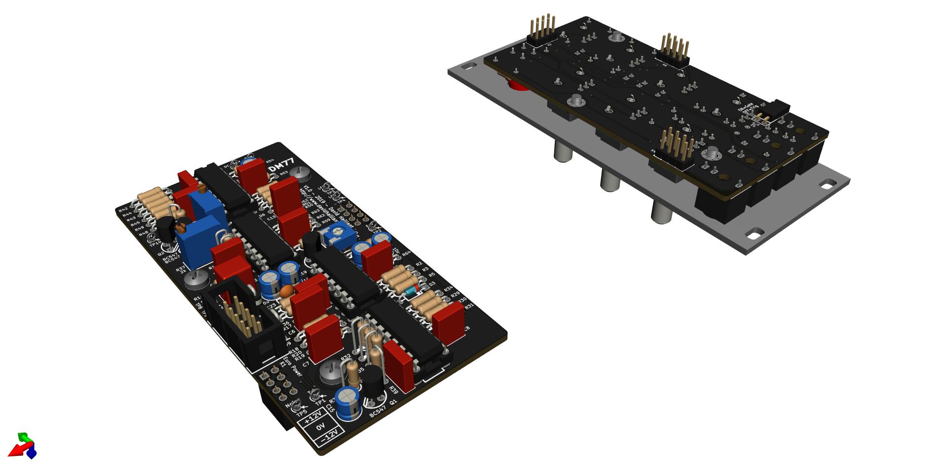
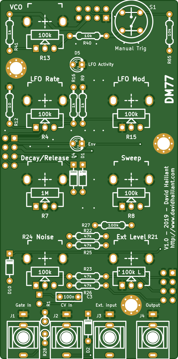
There is two boards:
- The first is for the user controls (the potentiometers, the jack sockets, the two LEDs and the trigger button) and is located right behind the front panel. This board can be refereed to as Board A.
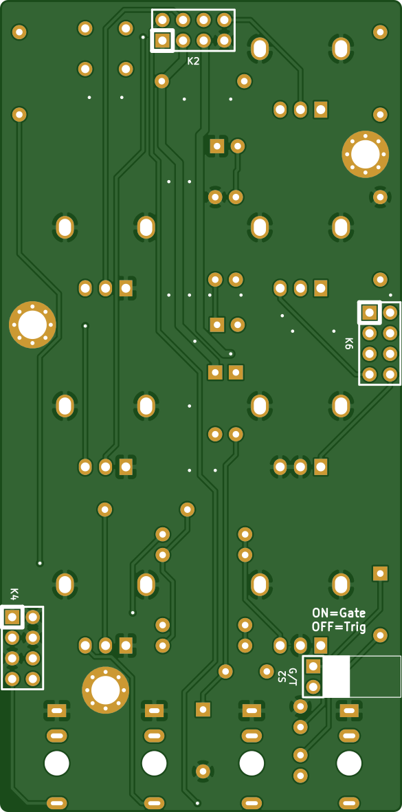
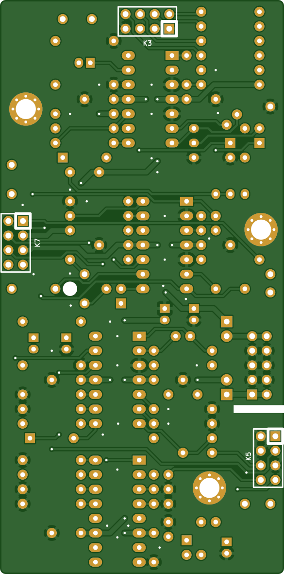
- The second board (Board B) is the most populated and is located at the back of the module. Board B is oriented differently from the Board A: the components face the rear. There’s no component – except the interconnection connectors, and the Gate/Trig jumper selector (S2) between the two boards.
Depending on the chosen interconnect solution, the two boards are roughly 11mm spaced.
The best practice is to start by soldering the small components: the resistors (horizontal mounting*), the small diodes, then the IC supports, followed by the bigger, taller components: ceramic/plastic capacitors, vertically mounted resistors and diodes, and the power input connector.
*: There’s two kind of resistor mounting: horizontal and vertical. The vertical mounting allow for a more compact design.
Note that resistor R46 is the Tempco. It is mounted close to the transistor pair Q2 and Q3 and should be in contact with them to ensure a good thermal coupling. Add some thermal grease, or any other low thermal resistance bounding material to improve the contact and heat transfer. You can also add a heat shrink tube around the three components, some foam, or any wrapping material you may like.
It is easier to solder R46 after Q2 and Q3, or, try to first tie the three components before soldering them all together.
The board interconnections are to be soldered on opposite sides from components’. Therefore, you need to pay attention to not damage surrounding components while soldering them. To this extent, it is advised to solder them early.
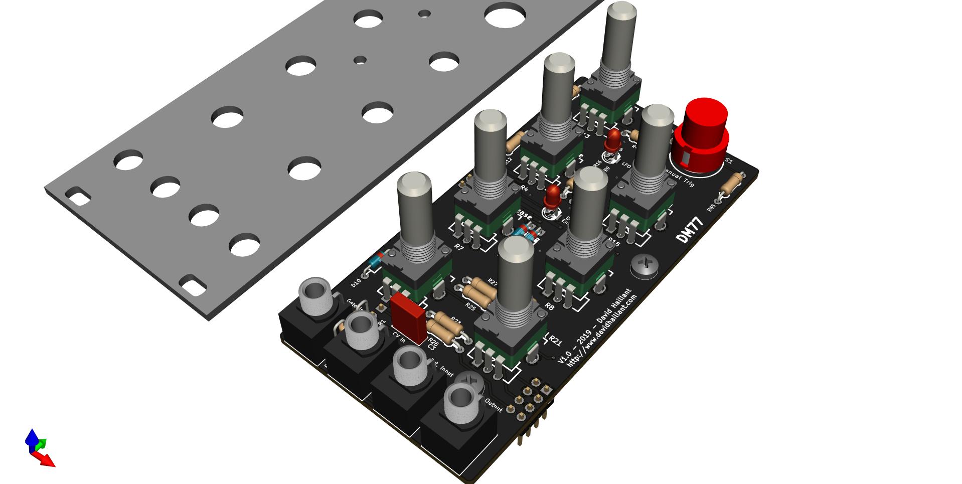
I recommend to solder the controls (potentiometers) and the jack connectors after they have been securely bolt in place to the front panel. Also use the front panel for a good alignment of the LEDs.
The potentiometers must have their protruding tabs removed before they get installed.
D8 and D9
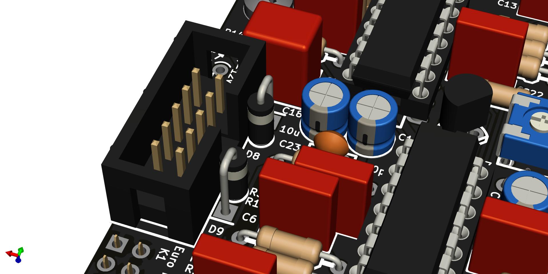
The diodes D8 and D9 are protection diodes against reversed power supply connectors. They are mounted vertically, with the “cathode up” which means, if you place the diode over the circle, the cathode is facing upward. The cathode is indicated with the white thick painted ring on the diode body.
Calibration and first tests
Powering on
Once you think you’ve soldered everything correctly, before powering your module for the first time, check twice that you haven’t put the ICs backward and that the power input connector is correctly oriented, and your power cable is trust worthy!
Furthermore, I recommend to power the module the first time without any IC inserted and check with a multimeter the presence of the expected voltage rails on the correct pins.
VCO calibration
The calibration process is identical to any other VCO. The 10 turn trim potentiometer R47 sets the 1V/Octave conformance.
The second 10 turn trim potentiometer, R37, is the setting for the high frequency compensation.
The required tools are:
- An accurate voltage source, capable of delivering a CV in 1V steps (0V, 1V, 2V, etc.) MIDI to CV modules are great for this.
- A frequency meter or a tuner.
- A small flat blade screw driver.
- Your tongue at righ angle and some patience.
- Also a multimeter, because you always need a multimeter.
- And if you have an oscilloscope, it’s a good idea to monitor the waveforms.
R37 must be set first to the lowest resistance between pin 1 and 3. It’s in full Counter Clockwise position.
Modulation potentiometers R8 and R15 (Sweep and FM Mod) must be turned off (Full Counter Clockwise). Noise also must be turned off (CCW)
If you read the signal at the main output, or use a tuner, you should set jumper link S2 on closed position and set Release potentiometer on Full Clockwise (longest release).
You can also read the main oscillator frequency from Test Points TP6, TP7 and TP1.
- The first step is to apply no CV input (0V) and turn the potentiometer R13 to set the main oscillator frequency at a low value. If you use a frequency meter, you can set the frequency to an easy-to-read value of 100Hz, for example. If you’re using a tuner, or your ears, tune the main oscillator to precisely A2 (110Hz).
- Then apply a 1V source on the CV input. The frequency of the main oscillator should double (200Hz or A3). If the frequency is flat, then adjust the trim potentiometer R47 and make the frequency go a bit flatter. If the frequency is sharp, then adjust R47 to get a frequency a bit sharper.
- Go back to 0V on CV input. Now the frequency is no more 100Hz (or A2). Adjust R13 back to 100Hz precisely (or A2).
- Repeat step 2, until the frequency doubles exactly when 1V is applied to the CV input.
- You can then check if the VCO frequency doubles again with a CV at 2V. The frequency must be 4x the base frequency (400Hz or A4).
- Do the same for 3V, 4V, etc. The frequency must double for each volt added on the CV input.
- At a certain point, the frequency will start to flatten, no matter how precisely you tuned the VCO on the lower octaves. You now need to adjust the second trim potentiometer R37. Turn clockwise R37 to increase the frequency. Once you’re back in tune, return to step 2 and start over.
After a number of iterations, the VCO is able to stay in tune for several octaves. The number of in-tune octaves depends on several factors. The quality of the transistors, among others. The matching of the transistors has no relation to how well the VCO will track. It only corrects the frequency drifts caused by temperature changes.
Waveshaper Calibration
The potentiometer R60 allow you to precisely remove the remaining artifacts from the saw to triangle conversion. By adjusting this potentiometer, you can remove the remaining high frequency harmonics still present. You can keep those harmonics if you prefer the harshness of the sound, or remove them completely to get a mellow triangle waveform.
Other measurements
Here are some more readings of the various Test Points.
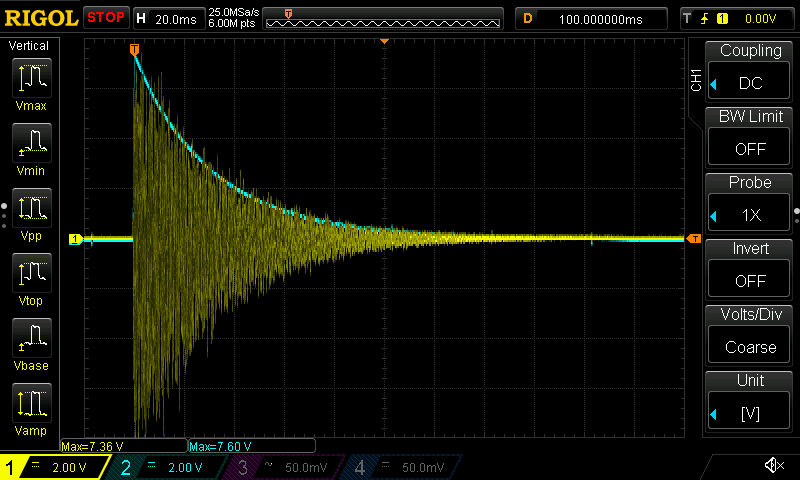
In blue: “Env” signal at TP2
More to come.
Downloads and documentation
- Schematics (dm77-1.0-20200117.pdf)
- Interactive BOM (dm77-1.0-ibom-2019-11-26-20200908)
- Online Spreadsheet BOM
- Front panel CAD files (dm77-10hp-20190312.zip)
Just finished building this. Tested all voltages before inserting the ICs. All good. Inserted the ICs, all works perfectly! I can get kick, snare, short hihat, melodic toms and anything else! Even an 808 style cowbell by using the LFO and FM. Brilliant module! Will start on calibration tomorrow!
Hello Richard and Thank you!
Glad you like the DM77!
Cheers!
hi, received this pcb set last friday,, i like it a lot, ive built a few drum circuits over the years, usually been disappointed, don’t really use drum sounds a lot, but this one does go beyond basics, crying out for a breakout module though !.. thinking simple vcf for noise, envelope out, saw out and lfo outputs, and most of these are easily taken from the test points, brilliant. very pleased, well thought out and even the panel is nice, doesn’t look like the usual pcb type panels
Hello Mark, thank you very much for your kind words and I’m really happy to know you like this module!
Your idea of a breakout module for some of the test points you mention is neat, I’ll have a look at it.
Have fun!