
The Attenuator – Inverter “Chicklet” is a compact, single-channel utility PCB derived from the AttenuVerter. It attenuates and/or inverts a voltage signal (CV or audio). All SMD components come pre-soldered; only the potentiometer (THT) and the connector need to be added.
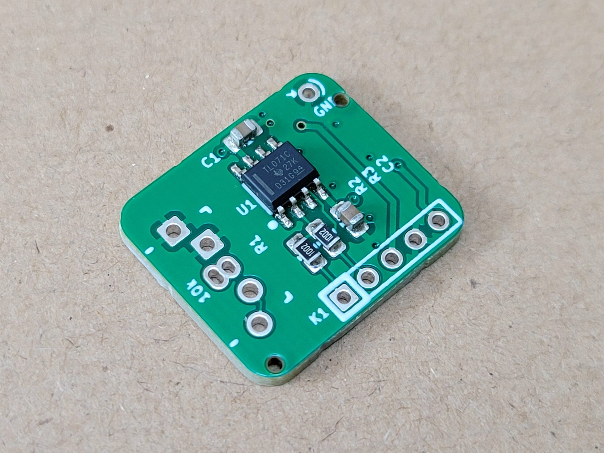
At only 22.225 mm × 19.05 mm, the Chicklet is designed to slip into an existing project with minimal effort. The board accepts either a 9 mm potentiometer (2.54 mm / 0.1″ pitch) or a 16 mm potentiometer (5.08 mm / 0.2″ pitch), depending on what fits your build.

Features
- Single-channel attenuator and inverter
- Very small footprint: 22.225 mm × 19.05 mm
- Easy integration into any existing project or enclosure
- All SMD components factory pre-soldered
- Only one THT part to solder: the potentiometer
- Compatible with 9 mm pots (2.54 mm pitch) or 16 mm pots (5.08 mm pitch)
- ±12 V power supply (±9 V to ±15 V range)
How it works
The circuit implements a simple gain stage around a single TL071 op-amp (U1). The potentiometer (R1) continuously varies the output multiplier α between −1 and +1:
Vout = α × Vin
| Cursor position | Multiplier (α) | Effect |
|---|---|---|
| Full clockwise | +1 | Signal unchanged |
| Centre | 0 | Signal cancelled (null output) |
| Full anti-clockwise | −1 | Signal fully inverted |
Typical uses include:
- Reducing the amount of CV applied to a VCF cutoff or VCA envelope input
- Reversing an LFO (e.g. turning a rising ramp into a falling ramp)
- Inverting any bipolar audio or CV signal

Bill of Materials (BOM)
| Designation | Qty | Reference | Note |
|---|---|---|---|
| 1 µF 0805 SMD capacitor | 2 | C1, C2 | Pre-soldered |
| 10 kΩ 0805 SMD resistor | 2 | R2, R3 | Pre-soldered |
| TL071 SOIC-8 op-amp | 1 | U1 | Pre-soldered |
| 10 kΩ linear potentiometer: 9 mm (2.54 mm pitch) or 16 mm (5.08 mm pitch) | 1 | R1 | To solder (THT) |
| 5×1 pin connector (male or female) or bare wires | 1 | K1 | To solder (THT) |
Build instructions
All SMD components (C1, C2, R2, R3, U1) are already soldered on the PCB. You only need to add two through-hole parts:
- Potentiometer R1: The board accepts a 9 mm pot (2.54 mm / 0.1″ pin pitch) or a 16 mm pot (5.08 mm / 0.2″ pin pitch). Before soldering, remove the protruding alignment tab with pliers if it prevents the pot from sitting flat behind the panel. Insert and solder the three pins.
- Connector K1: Solder a 5-pin male or female header, or connect five bare wires directly (see wiring table below).


Connections
| Pin | Signal | Details |
|---|---|---|
| 1 | Input | Signal input, ±10 V max (for ±12 V supply) |
| 2 | Output | Processed signal output |
| 3 | +12 V | Positive supply (+15 V max) |
| 4 | GND | “Ground” or 0 V, common to signal and power |
| 5 | −12 V | Negative supply (−15 V max) |
The module requires a split (bipolar) power supply. It operates from ±9 V to ±15 V. The standard Eurorack ±12 V works perfectly. Keep input signals within ±10 V when powered at ±12 V; exceeding this will cause the op-amp to saturate.

Specifications
| Parameter | Value |
|---|---|
| PCB dimensions | 22.225 mm × 19.05 mm |
| Power supply | ±9 V to ±15 V (typically ±12 V) |
| Input voltage range | ±10 V max (at ±12 V supply) |
| Output multiplier range | −1 to +1 (continuous) |
| Op-amp | TL071 (SOIC-8) |
| Input impedance | Determined by R1 (10 kΩ pot) |
| Channels | 1 |
| Offset | None |